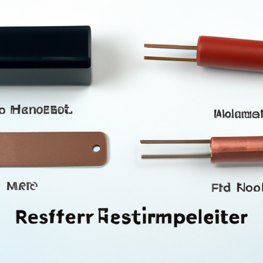
What Components and Modules Does a Thin Film Resistor Contain?

I. Introduction
Thin film resistors are essential components in modern electronic circuits, known for their precision and reliability. Unlike traditional resistors, which are often made from bulk materials, thin film resistors are fabricated by depositing a thin layer of resistive material onto a substrate. This unique construction allows for superior performance in various applications, making them a popular choice in high-precision environments. In this blog post, we will explore the components and modules that make up thin film resistors, delving into their structure, manufacturing processes, performance characteristics, and applications.
II. Basic Structure of Thin Film Resistors
A. Substrate Material
The substrate is the foundational layer upon which the resistive film is deposited. It plays a crucial role in the overall performance of the thin film resistor. Common substrate materials include ceramic, glass, and silicon. Each type of substrate offers distinct advantages:
1. **Ceramic**: Known for its excellent thermal stability and electrical insulation properties, ceramic substrates are widely used in high-temperature applications.
2. **Glass**: Glass substrates provide a smooth surface for film deposition and are often used in applications requiring high transparency and low thermal expansion.
3. **Silicon**: Silicon substrates are favored in integrated circuits due to their compatibility with semiconductor technology.
The choice of substrate material can significantly influence the resistor's performance, including its thermal characteristics and mechanical stability.
B. Resistive Film
The resistive film is the heart of the thin film resistor, determining its resistance value and performance characteristics. This layer is typically composed of metals or metal oxides, with common materials including nickel-chromium (NiCr), tantalum nitride (TaN), and indium tin oxide (ITO). The thickness of the resistive layer is critical; it directly impacts the resistance value, with thinner films generally resulting in higher resistance. The precise control of film thickness during manufacturing is essential for achieving the desired electrical properties.
C. Protective Coating
To enhance durability and protect the resistive film from environmental factors, a protective coating is often applied. This coating serves multiple purposes, including:
1. **Environmental Protection**: It shields the resistive layer from moisture, dust, and chemical exposure, which can degrade performance over time.
2. **Mechanical Protection**: The coating provides a barrier against physical damage, ensuring the longevity of the resistor.
Common materials used for protective coatings include epoxy resins and silicone-based compounds, which offer excellent adhesion and resistance to environmental stressors.
III. Key Components of Thin Film Resistors
A. Terminals
Terminals are critical for establishing electrical connections between the thin film resistor and the circuit. There are various types of terminals, including solderable and wire-bondable options. The design of the terminals is crucial, as it affects the ease of integration into circuits and the overall reliability of the connection. Proper terminal design ensures minimal resistance at the connection points, which is vital for maintaining the accuracy of the resistor.
B. Contact Pads
Contact pads are the areas on the resistor where electrical connections are made. They play a vital role in ensuring reliable electrical contact with the circuit. The materials used for contact pads are typically chosen for their conductivity and compatibility with the resistive film. Common materials include gold, silver, and copper, each offering different advantages in terms of conductivity and corrosion resistance.
C. Passivation Layer
The passivation layer is an additional protective layer applied to the thin film resistor. Its primary purpose is to prevent oxidation and contamination of the resistive film, which can adversely affect performance. The passivation layer is typically made from materials such as silicon dioxide (SiO2) or silicon nitride (Si3N4). The application of this layer is crucial for enhancing the stability and reliability of the resistor over time.
IV. Manufacturing Process of Thin Film Resistors
A. Deposition Techniques
The manufacturing of thin film resistors involves several key processes, starting with the deposition of the resistive film. Two primary techniques are used:
1. **Physical Vapor Deposition (PVD)**: This method involves the physical transfer of material from a solid source to the substrate in a vacuum environment. PVD techniques, such as sputtering and evaporation, allow for precise control over film thickness and composition.
2. **Chemical Vapor Deposition (CVD)**: In CVD, gaseous precursors react chemically to form a solid film on the substrate. This technique is particularly useful for creating uniform coatings and can be used to deposit a variety of materials.
B. Patterning Techniques
Once the resistive film is deposited, it must be patterned to create the desired resistor shape. This is typically achieved through photolithography, where a light-sensitive photoresist is applied to the film. The photoresist is then exposed to UV light through a mask, and the unexposed areas are removed, leaving behind the desired pattern. Following this, etching processes are used to remove excess material, finalizing the resistor's shape.
C. Quality Control Measures
Quality control is paramount in the manufacturing of thin film resistors. Testing for resistance values is conducted to ensure that each resistor meets specified tolerances. Additionally, environmental testing is performed to assess the resistor's performance under various conditions, such as temperature fluctuations and humidity. These measures help ensure the reliability and longevity of the resistors in their intended applications.
V. Performance Characteristics
A. Temperature Coefficient of Resistance (TCR)
The Temperature Coefficient of Resistance (TCR) is a critical performance characteristic of thin film resistors. It measures how much the resistance changes with temperature. A low TCR is desirable for precision applications, as it indicates that the resistor will maintain its resistance value over a range of temperatures. Factors affecting TCR include the materials used in the resistive film and the substrate's thermal properties.
B. Stability and Reliability
Stability and reliability are essential for thin film resistors, especially in applications where precision is crucial. Long-term performance is influenced by factors such as environmental conditions, mechanical stress, and the quality of the materials used. Environmental resistance, including resistance to moisture and temperature variations, is also a key consideration in the design and manufacturing process.
C. Noise Characteristics
Noise is an inherent characteristic of all resistors, and thin film resistors are no exception. Various types of noise can affect circuit performance, including thermal noise and flicker noise. Understanding the noise characteristics of thin film resistors is vital for engineers, as it can impact the overall performance of sensitive electronic circuits.
VI. Applications of Thin Film Resistors
Thin film resistors find applications across a wide range of industries due to their precision and reliability. Some notable applications include:
A. Use in Precision Measurement Devices
Thin film resistors are commonly used in precision measurement devices, such as digital multimeters and oscilloscopes. Their low TCR and high stability make them ideal for applications requiring accurate measurements.
B. Role in Integrated Circuits
In integrated circuits, thin film resistors are often used for biasing and feedback applications. Their small size and precise resistance values allow for efficient circuit design and improved performance.
C. Applications in Automotive and Aerospace Industries
The automotive and aerospace industries demand high-performance components that can withstand extreme conditions. Thin film resistors are used in various applications, including sensor systems, control units, and navigation systems, where reliability and precision are paramount.
VII. Conclusion
In summary, thin film resistors are complex components that play a vital role in modern electronic circuits. Their unique structure, comprising a substrate, resistive film, protective coating, terminals, contact pads, and passivation layer, contributes to their superior performance. The manufacturing processes, including deposition and patterning techniques, ensure that these resistors meet stringent quality standards. With their excellent performance characteristics, thin film resistors are widely used in precision measurement devices, integrated circuits, and critical applications in the automotive and aerospace industries.
As technology continues to advance, the demand for high-precision components like thin film resistors will only grow. Understanding the design and functionality of these resistors is essential for engineers and designers working in the field of electronics, as it enables them to create more efficient and reliable circuits. The future of thin film resistor technology promises exciting developments, including new materials and manufacturing techniques that will further enhance their performance and applicability in various industries.
What Components and Modules Does a Thin Film Resistor Contain?

I. Introduction
Thin film resistors are essential components in modern electronic circuits, known for their precision and reliability. Unlike traditional resistors, which are often made from bulk materials, thin film resistors are fabricated by depositing a thin layer of resistive material onto a substrate. This unique construction allows for superior performance in various applications, making them a popular choice in high-precision environments. In this blog post, we will explore the components and modules that make up thin film resistors, delving into their structure, manufacturing processes, performance characteristics, and applications.
II. Basic Structure of Thin Film Resistors
A. Substrate Material
The substrate is the foundational layer upon which the resistive film is deposited. It plays a crucial role in the overall performance of the thin film resistor. Common substrate materials include ceramic, glass, and silicon. Each type of substrate offers distinct advantages:
1. **Ceramic**: Known for its excellent thermal stability and electrical insulation properties, ceramic substrates are widely used in high-temperature applications.
2. **Glass**: Glass substrates provide a smooth surface for film deposition and are often used in applications requiring high transparency and low thermal expansion.
3. **Silicon**: Silicon substrates are favored in integrated circuits due to their compatibility with semiconductor technology.
The choice of substrate material can significantly influence the resistor's performance, including its thermal characteristics and mechanical stability.
B. Resistive Film
The resistive film is the heart of the thin film resistor, determining its resistance value and performance characteristics. This layer is typically composed of metals or metal oxides, with common materials including nickel-chromium (NiCr), tantalum nitride (TaN), and indium tin oxide (ITO). The thickness of the resistive layer is critical; it directly impacts the resistance value, with thinner films generally resulting in higher resistance. The precise control of film thickness during manufacturing is essential for achieving the desired electrical properties.
C. Protective Coating
To enhance durability and protect the resistive film from environmental factors, a protective coating is often applied. This coating serves multiple purposes, including:
1. **Environmental Protection**: It shields the resistive layer from moisture, dust, and chemical exposure, which can degrade performance over time.
2. **Mechanical Protection**: The coating provides a barrier against physical damage, ensuring the longevity of the resistor.
Common materials used for protective coatings include epoxy resins and silicone-based compounds, which offer excellent adhesion and resistance to environmental stressors.
III. Key Components of Thin Film Resistors
A. Terminals
Terminals are critical for establishing electrical connections between the thin film resistor and the circuit. There are various types of terminals, including solderable and wire-bondable options. The design of the terminals is crucial, as it affects the ease of integration into circuits and the overall reliability of the connection. Proper terminal design ensures minimal resistance at the connection points, which is vital for maintaining the accuracy of the resistor.
B. Contact Pads
Contact pads are the areas on the resistor where electrical connections are made. They play a vital role in ensuring reliable electrical contact with the circuit. The materials used for contact pads are typically chosen for their conductivity and compatibility with the resistive film. Common materials include gold, silver, and copper, each offering different advantages in terms of conductivity and corrosion resistance.
C. Passivation Layer
The passivation layer is an additional protective layer applied to the thin film resistor. Its primary purpose is to prevent oxidation and contamination of the resistive film, which can adversely affect performance. The passivation layer is typically made from materials such as silicon dioxide (SiO2) or silicon nitride (Si3N4). The application of this layer is crucial for enhancing the stability and reliability of the resistor over time.
IV. Manufacturing Process of Thin Film Resistors
A. Deposition Techniques
The manufacturing of thin film resistors involves several key processes, starting with the deposition of the resistive film. Two primary techniques are used:
1. **Physical Vapor Deposition (PVD)**: This method involves the physical transfer of material from a solid source to the substrate in a vacuum environment. PVD techniques, such as sputtering and evaporation, allow for precise control over film thickness and composition.
2. **Chemical Vapor Deposition (CVD)**: In CVD, gaseous precursors react chemically to form a solid film on the substrate. This technique is particularly useful for creating uniform coatings and can be used to deposit a variety of materials.
B. Patterning Techniques
Once the resistive film is deposited, it must be patterned to create the desired resistor shape. This is typically achieved through photolithography, where a light-sensitive photoresist is applied to the film. The photoresist is then exposed to UV light through a mask, and the unexposed areas are removed, leaving behind the desired pattern. Following this, etching processes are used to remove excess material, finalizing the resistor's shape.
C. Quality Control Measures
Quality control is paramount in the manufacturing of thin film resistors. Testing for resistance values is conducted to ensure that each resistor meets specified tolerances. Additionally, environmental testing is performed to assess the resistor's performance under various conditions, such as temperature fluctuations and humidity. These measures help ensure the reliability and longevity of the resistors in their intended applications.
V. Performance Characteristics
A. Temperature Coefficient of Resistance (TCR)
The Temperature Coefficient of Resistance (TCR) is a critical performance characteristic of thin film resistors. It measures how much the resistance changes with temperature. A low TCR is desirable for precision applications, as it indicates that the resistor will maintain its resistance value over a range of temperatures. Factors affecting TCR include the materials used in the resistive film and the substrate's thermal properties.
B. Stability and Reliability
Stability and reliability are essential for thin film resistors, especially in applications where precision is crucial. Long-term performance is influenced by factors such as environmental conditions, mechanical stress, and the quality of the materials used. Environmental resistance, including resistance to moisture and temperature variations, is also a key consideration in the design and manufacturing process.
C. Noise Characteristics
Noise is an inherent characteristic of all resistors, and thin film resistors are no exception. Various types of noise can affect circuit performance, including thermal noise and flicker noise. Understanding the noise characteristics of thin film resistors is vital for engineers, as it can impact the overall performance of sensitive electronic circuits.
VI. Applications of Thin Film Resistors
Thin film resistors find applications across a wide range of industries due to their precision and reliability. Some notable applications include:
A. Use in Precision Measurement Devices
Thin film resistors are commonly used in precision measurement devices, such as digital multimeters and oscilloscopes. Their low TCR and high stability make them ideal for applications requiring accurate measurements.
B. Role in Integrated Circuits
In integrated circuits, thin film resistors are often used for biasing and feedback applications. Their small size and precise resistance values allow for efficient circuit design and improved performance.
C. Applications in Automotive and Aerospace Industries
The automotive and aerospace industries demand high-performance components that can withstand extreme conditions. Thin film resistors are used in various applications, including sensor systems, control units, and navigation systems, where reliability and precision are paramount.
VII. Conclusion
In summary, thin film resistors are complex components that play a vital role in modern electronic circuits. Their unique structure, comprising a substrate, resistive film, protective coating, terminals, contact pads, and passivation layer, contributes to their superior performance. The manufacturing processes, including deposition and patterning techniques, ensure that these resistors meet stringent quality standards. With their excellent performance characteristics, thin film resistors are widely used in precision measurement devices, integrated circuits, and critical applications in the automotive and aerospace industries.
As technology continues to advance, the demand for high-precision components like thin film resistors will only grow. Understanding the design and functionality of these resistors is essential for engineers and designers working in the field of electronics, as it enables them to create more efficient and reliable circuits. The future of thin film resistor technology promises exciting developments, including new materials and manufacturing techniques that will further enhance their performance and applicability in various industries.


